Schematic & PCB design
An EDA tool your agent can actually drive
Schema is a desktop schematic and PCB editor where every capability — placement, routing, copper pours, design-rule checks, fabrication output — is exposed identically to you and to an AI agent. No scripting bridge, no plugin shim. The same commands either way.
The whole loop, in one tool
Most EDA automation is bolted on after the fact. Schema was built the other way round.
Schematic to fabrication
Capture a schematic, push the netlist to a board, place footprints, route the copper, pour the ground plane, and export Gerber and Excellon drill files.
An agent surface, not a macro language
A command layer built for perceive / act / verify / recover: an agent can describe the board, make a change, run DRC, look at a render, and undo when it gets it wrong.
Your existing libraries
Reads KiCad symbol and footprint libraries and Altium schematic libraries directly. Point Schema at the parts you already have and keep working.
Rules checked as you go
Clearance, annular ring, edge clearance, unconnected nets and silkscreen conflicts are checked against per-net-class rules, with every violation placed on the board.
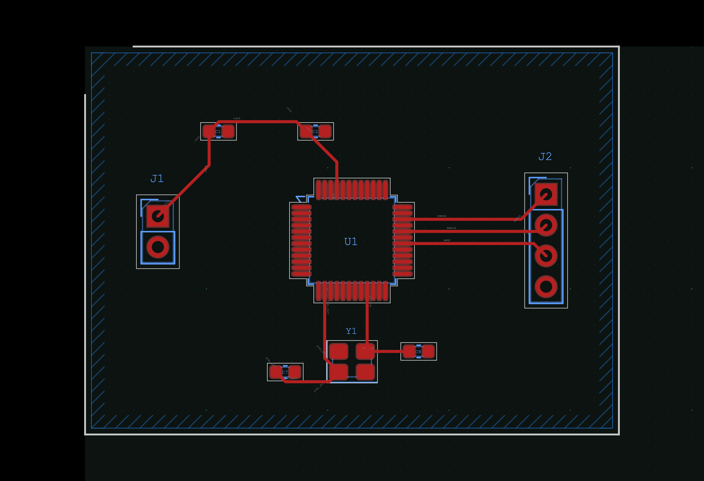
PCB editor
Layout that holds its own rules
Place footprints from your libraries, route with walk-around collision handling, and pour copper that respects pad clearances the way a fabricator expects.
- Interactive routing with 45° and orthogonal constraints, vias, and net-class track widths
- Zone fill with per-pad clearance, thermal-relief settings and island removal
- Live ratsnest and joint-based connectivity as the board changes
- Gerber RS-274X and Excellon drill export, including plated and non-plated splits
Built for the work, not the demo
Schema is in active development. Here is what the editor does today.
- Schematic capture
- KiCad + Altium symbol libraries
- Board layout
- footprints, outlines, silkscreen
- Interactive routing
- walk-around, 45° / orthogonal
- Copper pours
- clearance-accurate zone fill
- Design-rule checks
- per-net-class constraints
- Fabrication output
- Gerber RS-274X, Excellon, SVG